
Engineering Precision
at Scale
Our patented and innovative technology enables a mechanical precision imprint process that defines conductive structures through precision mechanical structuring, combining scientific rigor with scalable manufacturing.
The Technology Story
From Science to Industrial Platform
Origin & Scientific Foundation
DP Patterning originates from advanced research within material science and manufacturing technologies, with the ambition to challenge conventional etching and printed electronics. The core idea was to replace complex chemical processes with a precise, mechanical method—enabling cleaner, more efficient production of conductive structures.
Developed as a spin-off from Research Institutes of Sweden (RISE), the technology builds on decades of research and industrial insight, forming the foundation for a new generation of electronics manufacturing.
The Physics Behind the Process
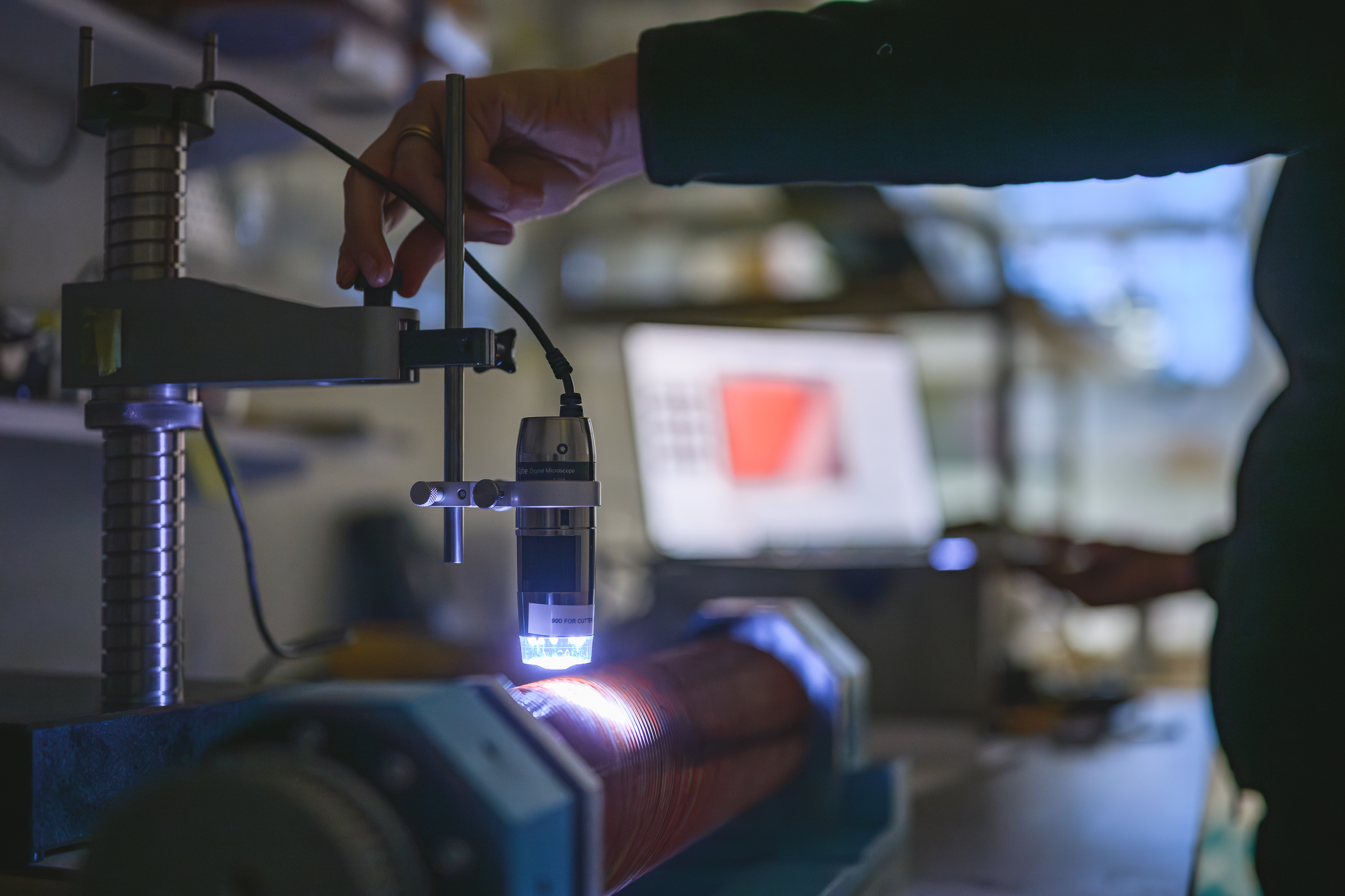
At the core of Dry Phase Patterning lies a mechanical precision imprint process, where conductive patterns are formed through precision mechanical/cutting structuring rather than chemical removal or ink deposition.
This results in solid-metal conductors with superior electrical properties compared to printed alternatives, while eliminating variability associated with inks, solvents, and curing processes. The outcome is a stable, repeatable structure with high conductivity and long-term reliability.
Compared to traditional etching, Dry Phase Patterning avoids chemical material removal, reducing waste, process variation, and overall complexity with fewer process steps. It also eliminates issues such as underetch, enabling sharper feature definition and more stable geometries.
Process Architecture
The technology is designed as a continuous roll-to-roll process, enabling high-throughput manufacturing with consistent precision. Each step in the process is engineered for stability, repeatability, and control—ensuring uniform quality across large volumes.
Unlike batch-based methods, this architecture allows for efficient scaling while maintaining tight tolerances and predictable performance.
From Lab to Machines to Industrial Scale
DP Patterning has taken full ownership of its technology journey—from early research and prototyping to the development of proprietary manufacturing equipment.
By designing and building our own machines, we have translated scientific principles into a robust, industrial platform. While initially exploring machine commercialization, we made a strategic decision to focus on what creates the greatest value: producing flexible electronics at scale.
Today, this results in a fully integrated manufacturing capability—combining deep process knowledge with industrial execution, and enabling reliable, high-volume production.
This positions DP Patterning as a unique partner for companies seeking a cost-efficient and truly sustainable alternative to conventional electronics production—without compromising on performance or scalability.
Engineering Excellence
The Team Behind the Technology
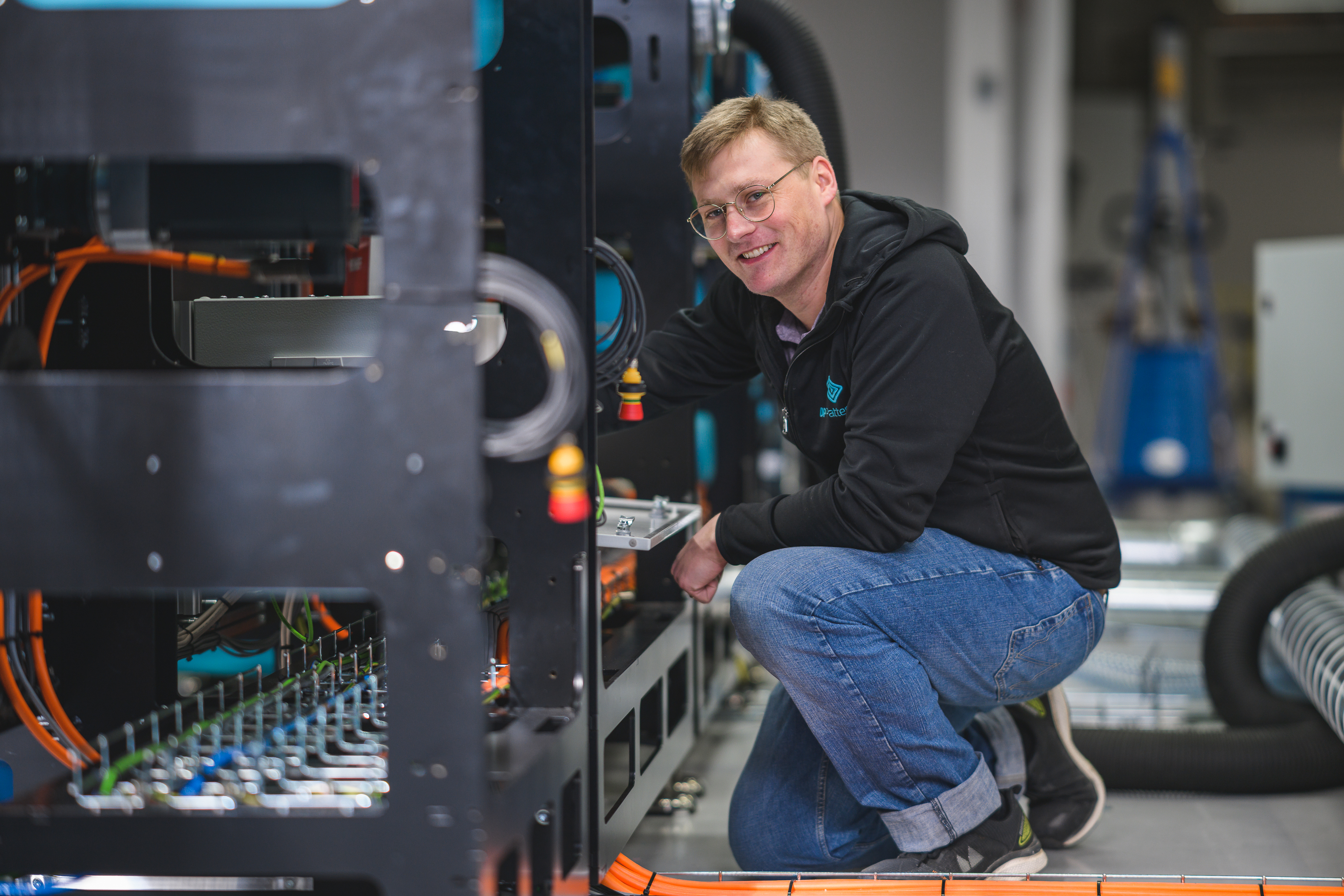
Behind DP Patterning stands a team of highly specialized engineers and developers with deep expertise in materials science, process technology, and industrial manufacturing. The team combines strong capabilities in electrical design and engineering, software development, industrial automation, quality assurance, mechanical design, metrology, and advanced analysis.
In addition, DP Patterning has extensive expertise in printed electronics and the development of scalable manufacturing solutions for flexible electronic applications.
This includes world-class competencies, where individual expertise represents capabilities found in only a handful of experts globally.
This knowledge is embedded in every step of the technology — from process development to machine design and production — ensuring precision, performance and continuous innovation.
Core Competencies
Discuss the Science with Our Experts
Our technology is developed and led by senior scientists and industrial engineers with deep expertise in nanoimprint lithography, materials science, and scalable manufacturing.
Roman Armgarth, PhD
CTO
Direct access to the scientists and engineers who designed and built the platform. No sales layer — just technical depth.